Laboratory of nanomagnetism
The functional characterization of our materials and devices takes place in our laboratory of nanomagnetism of the Department of Physics, which is equipped for magnetic, optical and electrical testing.
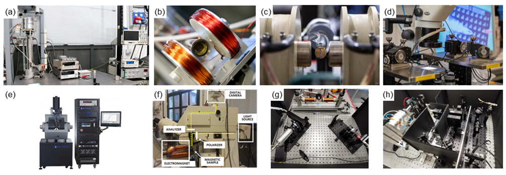
For the magnetic characterization, the lab is equipped with a vibrating sample magnetometer, two setups for magneto-optical Kerr effect measurements (also with spacial resolutio) and a magneto-optical microscope for domain imagining.
For electrical characterization, we are equipped with a standard closed-loop cryostat (<10 K) with optical and electrical access; a cryogenic four probe system; a couple of table-top four probe systems operating at room temperature; a custom system to measure the electric properties of bonded devices within magnetic fields; standard Keithley sourcemeters, nanovoltmeters, current source, multimeters and lock-in amplifiers by Zurich Instruments. Additionally, we have the possibility to carefully measure the response of devices in a cryostat for low temperatures (1.6 K) and high magnetic fields (7 T) at the Department of Physics.
For ferroelectric characterization, we are equipped with a thin film analyser TFA 2000 (by AixAct Gmbh) able to measure ferroelectric hysteresis loops, retention, leakage, dielectric constant, with a temporal resolution of 250 ns.
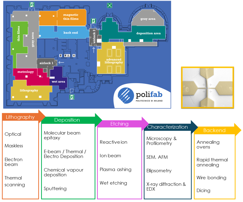
Polifab
Our activity is centred in Polifab (www.polifab.polimi.it), which has a cleanroom of about 620 m2 (Figure 16) and will expand to more than 1200 m2 by 2026 in the new technological pole in Bovisa La Goccia.
Polifab is an open infrastructure providing the highest technological standards for a wide range of applications and processes involving all the Key Enabling Technologies (photonics, micro and nanoelectronics, biotechnologies, advanced materials and nanotechnology).
Through Polifab, we have access to expensive instrumentation allowing us to fulfil the complete workflow of our processes (from materials growth to the realization of devices). In particular, state-of-art lithographic processes using maskless optical lithography, thermally-assisted scanning probe and electron beam lithography. All these tools are supported by additive (deposition) and subtractive (etching) techniques to transfer the desired design to an actual electronic device (see the figure below and find more details on the official website of the facility at www.polifab.polimi.it).